%20--%3e%3csvg%20version='1.1'%20id='图层_1'%20xmlns='http://www.w3.org/2000/svg'%20xmlns:xlink='http://www.w3.org/1999/xlink'%20x='0px'%20y='0px'%20viewBox='0%200%20289.2%2071.5'%20style='enable-background:new%200%200%20289.2%2071.5;'%20xml:space='preserve'%3e%3cstyle%20type='text/css'%3e%20.st0{fill-rule:evenodd;clip-rule:evenodd;fill:%23B81C22;}%20.st1{fill:%23B81C22;}%20%3c/style%3e%3cg%3e%3cpath%20class='st0'%20d='M286.5,2.7c-0.2-0.5-0.7-1-1.6-1c-4.1,0-9.1,0-9.1,0c-2.9,0-6.1,3.1-6.1,3.1c0,0-13,14.6-21.8,23.4l-1,1%20l2.3-18.7c0.3-2.2-0.4-4.5-1.9-6.1c-1.5-1.7-3.6-2.7-5.9-2.7h-2.8c-1,0-1.8,0.7-1.9,1.7l-8.3,65.1c-0.1,0.5,0.1,1.1,0.5,1.5%20c0.4,0.4,0.9,0.7,1.4,0.7h3c4.8,0,8.8-3.5,9.4-8.3l1.8-14.2l6.6-6.6l0.3,0.5c3.5,5.3,16.2,24.4,16.9,25.6c0.4,0.4,1.9,3.1,6.2,3.1%20l8.6-0.1c0.8,0,1.4-0.4,1.7-1.1c0.3-0.7,0.3-1.4-0.1-2.1l-22.1-32.5c-1.2-1.7-1-4,0.5-5.5l23.1-24.8C286.7,3.9,286.7,3.2,286.5,2.7%20'/%3e%3cpath%20class='st0'%20d='M174.4,14.3C174.4,14.3,174.4,14.2,174.4,14.3L176,4c0.1-0.7-0.1-1.3-0.5-1.8c-0.4-0.5-1.1-0.8-1.8-0.8h-50.4%20c-1.5,0-3,1.2-3.2,2.7l-1.3,10.2h21.1l-7.1,56.2l13.1,0c0.1,0,0.1-0.1,0.1-0.1l7.4-56.2H174.4z'/%3e%3cpath%20class='st0'%20d='M13,1.4h-2.6c-0.9,0-1.8,0.8-1.9,1.7L0.8,64.4c-0.2,1.6,0.2,3,1.2,4.1c1,1.1,2.5,1.8,4.1,1.8h39.7%20c1.3,0,2.4-1,2.6-2.3c0.4-3-0.4-5.8-2.3-7.9c-1.9-2.1-4.6-3.3-7.6-3.3H23.7c-1.6,0-3.1-0.7-4.1-1.9c-1.1-1.2-1.5-2.8-1.3-4.3%20L23,12.7c0.4-3-0.4-5.8-2.3-8C18.8,2.6,16.1,1.4,13,1.4'/%3e%3cpath%20class='st0'%20d='M223,40.3c0.3,0,0.5-0.2,0.6-0.5l1.1-8.4c0-0.1,0-0.2-0.1-0.3c-0.1-0.1-0.1-0.1-0.3-0.1h-8%20c-0.3,0-0.5,0.2-0.6,0.5l-1.1,8.4c0,0.1,0,0.2,0.1,0.3c0.1,0.1,0.1,0.1,0.3,0.1H223z'/%3e%3cpath%20class='st0'%20d='M229,1.4h-35.4c-6.9,0-13.1,5.5-14,12.3L174,58c-0.4,3.3,0.5,6.4,2.6,8.7c2,2.3,4.9,3.6,8.2,3.6h35.8l0.5-5%20c0.2-2.1-0.5-4.1-1.9-5.7c-1.4-1.5-3.4-2.4-5.5-2.4l-17.2,0c-2.2,0-4.2-0.9-5.6-2.5c-1.4-1.6-2-3.7-1.8-6c0.6-4.5,4.7-8.3,9.3-8.3%20l11.5,0c0.3,0,0.6-0.2,0.6-0.5l1-8.3c0-0.1,0-0.2-0.1-0.3c-0.1-0.1-0.2-0.1-0.3-0.1l-11.6,0h0c-3.2,0-5.5-1.3-6.6-3.6%20c-1.3-2.8-1.1-6,0.6-8.6c1.8-2.8,4.8-4.5,8-4.5h18.1c4.5,0,8.3-3.3,8.8-7.8L229,1.4z'/%3e%3cpath%20class='st1'%20d='M112.3,9.9c-1.5-2.9-3.8-5.1-7-6.5c-3.1-1.4-7.4-2.1-12.8-2.1l-25.4,0h0c-2.5,0-4.8,2-5.1,4.5l-7.3,57.9%20c-0.2,1.8,0.3,3.4,1.4,4.7c1.1,1.3,2.7,1.9,4.5,1.9h23.5c4.5,0,8.4-0.4,11.6-1.2c3.2-0.8,6-1.9,8.3-3.5c2.3-1.5,4.4-3.8,6.2-6.6%20c1.8-2.8,2.9-5.9,3.3-9.1c0.5-4.1-0.2-7.6-2.2-10.6c-1.6-2.4-3.9-4.3-7-5.6l-0.9-0.4l0.9-0.5c2.5-1.4,4.6-3.2,6.1-5.3%20c2-2.7,3.2-5.5,3.6-8.5C114.4,15.9,113.8,12.8,112.3,9.9%20M101.5,21.7c-0.5,4-4,7.1-7.9,7.2H78.4l-0.2,1.3c-0.3,2.7,0.4,5.2,2.1,7.1%20c1.7,1.9,4.1,2.9,6.8,2.9h3.4c0.6,0,1.2,0.1,1.7,0.2c0.3,0,0.6,0.1,0.8,0.2l0,0.5l0.1-0.5c3.5,1.1,5.5,4.4,5.1,8.2%20c-0.6,4.6-4.8,8.4-9.5,8.4H71.4c-0.6,0-1.2-0.3-1.6-0.7c-0.4-0.5-0.6-1-0.5-1.6l4.9-38.6c0.1-1.1,1-1.8,2.1-1.8h0%20c15.3,0,18.2,0,18.8,0l0,0c1.9,0,3.7,0.8,4.9,2.1C101.2,17.9,101.7,19.7,101.5,21.7'/%3e%3c/g%3e%3c/svg%3e)
low-K Wafer Dicing
Silicon wafer — the "foundation" for manufacturing semiconductor integrated circuits. 6-inch and 8-inch wafers are being phased out, with 12-inch wafers becoming the mainstream. Larger wafer sizes lead to higher wafer utilization, lower chip production costs, and improved efficiency.
As wafer application specifications evolve, so do their processing methods. Previously, abrasive machining was used, but it suffered from low yield and unstable cutting profiles. This was later succeeded by mechanical dicing. However, directly processing low‑K wafers with mechanical dicing can cause metal chipping. Currently, laser grooving is gradually becoming the mainstream method, as it can remove the low‑K layer and relieve stress before mechanical dicing.
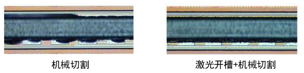
Comparison of Wafer Processing Methods (From Online)
Laser grooving mainly consists of three processing steps:
· Narrow Grooving: First, two fine protective grooves are cut inside the dicing street using the dual narrow laser method. This step determines whether the laser grooving process carries a risk of chipping.
· Wide Beam Grooving: The primary method for groove formation, which determines the groove profile and depth.
· After laser grooving is completed, a dicing blade is used to perform the full-cut processing.
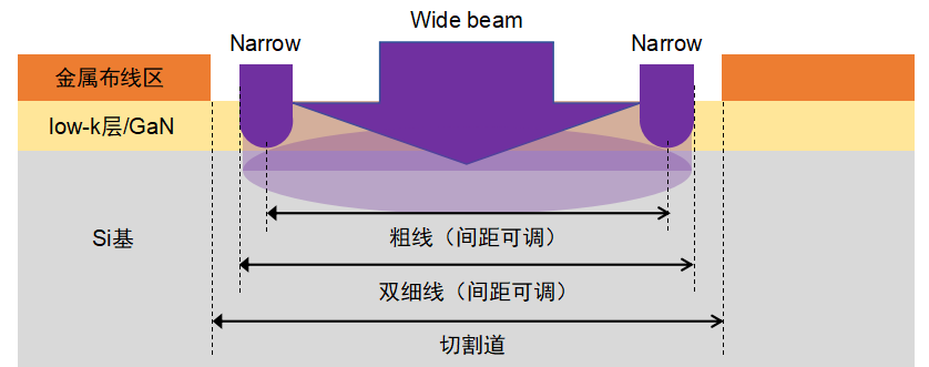
low-k晶圆开槽加工示意图
Regarding this process, LBTEK has introduced a low‑K wafer dicing solution, which addresses key challenges encountered during processing.
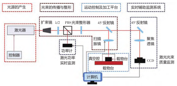
 Laser Grooving Optical Path for low-K Wafers
|
Key issues |
Important matters |
Measures |
|
Laser Control Method |
Power and pulse instability of long-pulse ultraviolet lasers |
Under a defined laser pulse, control the laser output using an optical beam-splitting method |
|
High-Precision Adjustable Beam Splitting Ratio |
A simple polarization beam splitting crystal cannot achieve high-precision adjustability |
By adding a half-wave plate and changing the polarization angle of the incident laser, high-precision adjustment of the beam splitting ratio can be achieved |
|
Adjustable Beam Splitting Spacing |
Different wafers require laser cutting of scribe lines with varying widths. The actual separation distance between the processed spots needs to range from 20 to 120 μm |
By adding a wedge prism into one of the beams and controlling the deflection of light, the beam splitting spacing can be adjusted |
|
Consistent Power of Split Beams |
The adjustable beam splitting achieved through deflection can cause differences in the power of the split beams, ultimately resulting in variations in the size and shape of the spots after splitting |
By adding a quarter-wave plate, linearly polarized light is converted into circularly polarized light. The electric field vector of circularly polarized light rotates uniformly, ensuring equal energy distribution in all directions |
|
Issue of Thermal Damage During Processing |
After focusing a Gaussian beam, the energy distribution of the spot is not uniform. The central region contains 86.5% of the total energy, while the remaining areas only account for 13.5% of the total energy. This leads to edge surface chipping and extensive heat-affected zones during processing |
By applying beam shaping technology, the Gaussian beam spot is transformed into a flat-top beam spot. This approach, on one hand, reduces thermal damage at the edges of the scribed lines, and on the other hand, ensures better flatness at the bottom of the scribed lines |
|
External Optical Path Alignment |
Laser grooving places high demands on spot quality, with a low tolerance for alignment errors |
More precise optical mounts and professional alignment techniques are employed |
LBTEK offers core components for laser grooving solutions for low-k wafers, including laser control modules, beam expansion and collimation modules, optical beam splitting modules, divergence and polarization control modules, relay lens modules, focusing and protection modules, optical switches, and more. Additionally, LBTEK provides comprehensive end-to-end service support, from conceptual design to practical implementation.
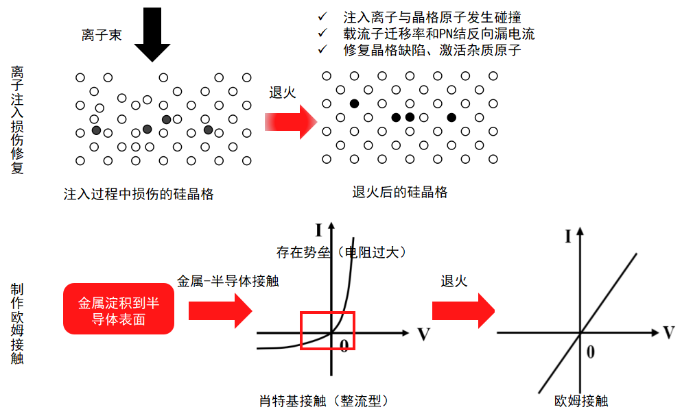
Laser Annealing
Annealing is a heat treatment process that involves heating a material to a specific temperature followed by controlled cooling. Two of its most critical applications in advanced manufacturing are repairing ion implantation damage and forming ohmic contacts. Selecting an appropriate annealing method is a key step in producing high-quality ohmic contacts for materials such as silicon carbide (SiC) and gallium nitride (GaN), enabling lower contact resistance and better stability. From the perspectives of wafer protection and energy efficiency, there is a demand for a localized wafer annealing process with shallow penetration depth.
Applications of Annealing(From Internet)
Traditional annealing processes are not ideal for repairing implantation damage. Even at temperatures as high as 1150°C, defects in the ion-implanted layer cannot be completely eliminated, and secondary defects are often generated. Additionally, these processes require long heat treatment durations, and significant impurity redistribution occurs during annealing. In contrast, laser annealing has emerged as the predominant annealing method due to its ability to perform localized annealing. The spot size and spatial positioning of the laser source in laser annealing are precisely controllable, enabling localized heating of the sample. With its high energy density, laser annealing significantly reduces annealing time. Post-annealing samples exhibit larger grain sizes, fewer defects, and the resulting devices demonstrate superior electrical performance.
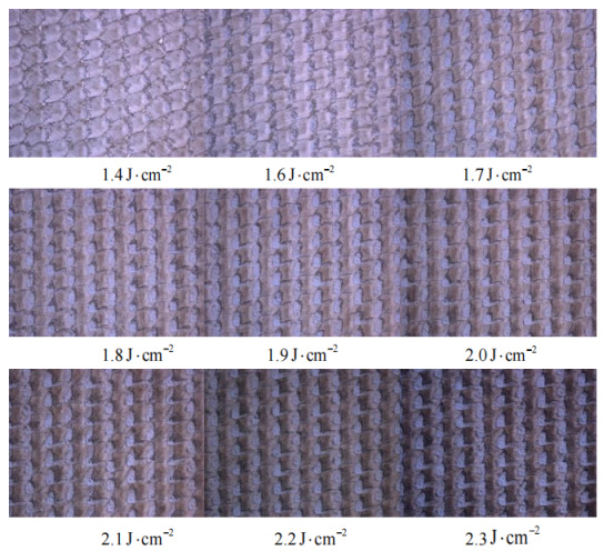 Optical micrographs of 4H-SiC under laser annealing at different energy densities(From Internet)
To address this process, LBTEK has introduced a laser annealing solution designed to resolve key challenges encountered during processing.
Laser Annealing Beam Path
|
Key issues |
Important matters |
Measures |
|
Laser Control Method |
Unstable power and pulse of pulsed ultraviolet lasers |
Under a defined laser pulse, the laser output is controlled and laser monitoring is achieved using an optical beam-splitting method involving a half-wave plate and a polarizing beam splitter (PBS) |
|
Inhomogeneous Laser Annealing Energy |
The original Gaussian beam spot exhibits uneven energy distribution |
A homogenizing diffractive optical element (DOE) is employed to improve the uniformity of the beam spot |
|
Adjustable Energy Density |
The energy density of the beam spot on the sample surface must reach the optimal energy density window |
An energy attenuator is used to achieve precise and continuous adjustment of the pulsed laser energy |
|
Achieving a High-Aspect-Ratio Line-Shaped Beam Spot |
For large-area samples, the beam spot morphology significantly impacts processing efficiency |
LBTEK provides core components for laser annealing solutions, including lasers, beam expansion and collimation modules, optical beam splitting modules, beam shaping modules, power detection modules, focusing and protection modules, and more. Additionally, LBTEK offers comprehensive end-to-end service support, from conceptual design to practical implementation.
Email: support@lbtek.com
Tel: 400-060-6986 (Mon-Sun 9:00-18:00)
 WeChat
 TikTok
 Zhihu
Zhihu Bilibili